- 您现在的位置:买卖IC网 > Sheet目录3850 > AT89C51RB2-3CSIM (Atmel)IC 8051 MCU FLASH 16K 40DIP
11
AT89C51RB2/RC2
4180E–8051–10/06
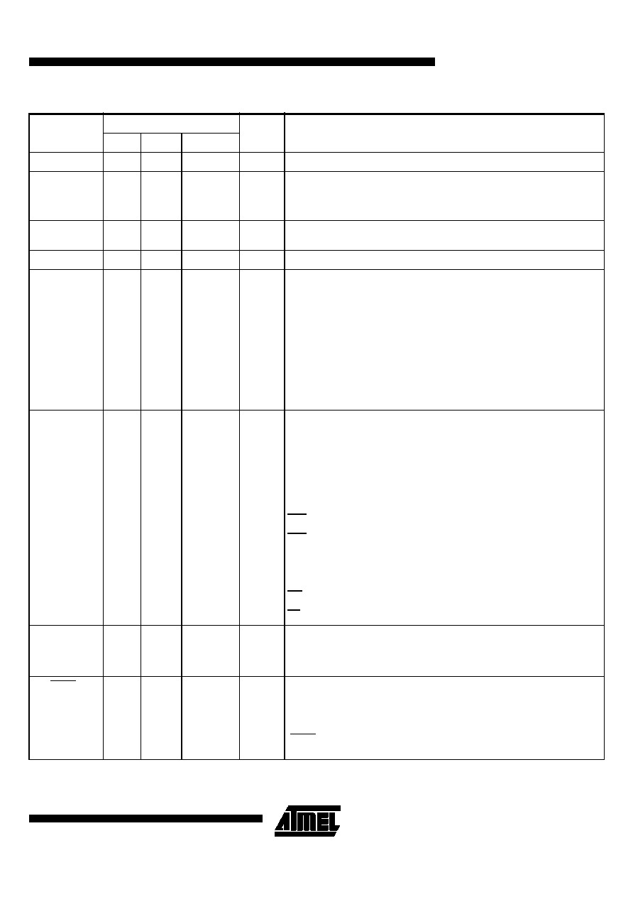
I/O
CEX4: Capture/Compare External I/O for PCA Module 4
P1.0 - P1.7
I/O
MOSI: SPI Master Output Slave Input line
When SPI is in master mode, MOSI outputs data to the slave peripheral. When SPI
is in slave mode, MOSI receives data from the master controller.
XTAL1
19
21
15
I
Crystal 1: Input to the inverting oscillator amplifier and input to the internal clock
generator circuits.
XTAL2
18
20
14
O
Crystal 2: Output from the inverting oscillator amplifier
P2.0 - P2.7
21 - 28
24 - 31
18 - 25
I/O
Port 2: Port 2 is an 8-bit bi-directional I/O port with internal pull-ups. Port 2 pins that
have 1s written to them are pulled high by the internal pull-ups and can be used as
inputs. As inputs, Port 2 pins that are externally pulled low will source current
because of the internal pull-ups. Port 2 emits the high - order address Byte during
fetches from external program memory and during accesses to external data
memory that use 16-bit addresses (MOVX @DPTR). In this application, it uses
strong internal pull-ups emitting 1s. During accesses to external data memory that
use 8-bit addresses (MOVX @Ri), port 2 emits the contents of the P2 SFR. Some
Port 2 pins receive the high order address bits during EPROM programming and
verification:
P2.0 to P2.5 for 16 KB devices
P2.0 to P2.6 for 32KB devices
P3.0 - P3.7
10 - 17
11,
13 - 19
5,
7 - 13
I/O
Port 3: Port 3 is an 8-bit bi-directional I/O port with internal pull-ups. Port 3 pins that
have 1s written to them are pulled high by the internal pull-ups and can be used as
inputs. As inputs, Port 3 pins that are externally pulled low will source current
because of the internal pull-ups. Port 3 also serves the special features of the
80C51 family, as listed below.
10
11
5
I
RXD (P3.0): Serial input port
11
13
7
O
TXD (P3.1): Serial output port
12
14
8
I
INT0 (P3.2): External interrupt 0
13
15
9
I
INT1 (P3.3): External interrupt 1
14
16
10
I
T0 (P3.4): Timer 0 external input
15
17
11
I
T1 (P3.5): Timer 1 external input
16
18
12
O
WR (P3.6): External data memory write strobe
17
19
13
O
RD (P3.7): External data memory read strobe
RST
9
10
4
I/O
Reset: A high on this pin for two machine cycles while the oscillator is running,
resets the device. An internal diffused resistor to VSS permits a power-on reset using
only an external capacitor to V
CC. This pin is an output when the hardware
watchdog forces a system reset.
ALE/PROG
30
33
27
O (I)
Address Latch Enable/Program Pulse: Output pulse for latching the low Byte of
the address during an access to external memory. In normal operation, ALE is
emitted at a constant rate of 1/6 (1/3 in X2 mode) the oscillator frequency, and can
be used for external timing or clocking. Note that one ALE pulse is skipped during
each access to external data memory. This pin is also the program pulse input
(PROG) during Flash programming. ALE can be disabled by setting SFR’s AUXR. 0
bit. With this bit set, ALE will be inactive during internal fetches.
Table 12. Pin Description for 40 - 44 Pin Packages (Continued)
Mnemonic
Pin Number
Type
Name and Function
DIL
LCC
VQFP44 1.4
发布紧急采购,3分钟左右您将得到回复。
相关PDF资料
PIC16C72A-04/SO
IC MCU OTP 2KX14 A/D PWM 28SOIC
AT89C51ID2-RLTIM
IC 8051 MCU FLASH 64K 44VQFP
AT89C51IC2-SLSIL
IC 8051 MCU FLASH 32K 44PLCC
AT89C51CC03U-RLTIM
IC 8051 MCU FLASH 64K 44VQFP
PIC24EP64MC204-I/PT
MCU 16BIT 64KB FLASH 44TQFP
AT89C51CC03U-RDTIM
IC 8051 MCU FLASH 64K 64VQFP
AT89C51CC03U-7CTIM
IC 8051 MCU FLASH 64K 64BGA
AT89C51CC03C-S3SIM
IC 8051 MCU FLASH 64K 52PLCC
相关代理商/技术参数
AT89C51RB2-3CSUL
功能描述:8位微控制器 -MCU 8-bit 16K Flash C51RB2 RoHS:否 制造商:Silicon Labs 核心:8051 处理器系列:C8051F39x 数据总线宽度:8 bit 最大时钟频率:50 MHz 程序存储器大小:16 KB 数据 RAM 大小:1 KB 片上 ADC:Yes 工作电源电压:1.8 V to 3.6 V 工作温度范围:- 40 C to + 105 C 封装 / 箱体:QFN-20 安装风格:SMD/SMT
AT89C51RB2-3CSUM
功能描述:8位微控制器 -MCU C51RB2 FLASH 5V 16k ind RoHS:否 制造商:Silicon Labs 核心:8051 处理器系列:C8051F39x 数据总线宽度:8 bit 最大时钟频率:50 MHz 程序存储器大小:16 KB 数据 RAM 大小:1 KB 片上 ADC:Yes 工作电源电压:1.8 V to 3.6 V 工作温度范围:- 40 C to + 105 C 封装 / 箱体:QFN-20 安装风格:SMD/SMT
AT89C51RB2L1-RLTUL
功能描述:8位微控制器 -MCU Microcontroller
RoHS:否 制造商:Silicon Labs 核心:8051 处理器系列:C8051F39x 数据总线宽度:8 bit 最大时钟频率:50 MHz 程序存储器大小:16 KB 数据 RAM 大小:1 KB 片上 ADC:Yes 工作电源电压:1.8 V to 3.6 V 工作温度范围:- 40 C to + 105 C 封装 / 箱体:QFN-20 安装风格:SMD/SMT
AT89C51RB2-RLRIL
功能描述:IC MCU FLASH 8051 16K 3V 44-VQFP RoHS:否 类别:集成电路 (IC) >> 嵌入式 - 微控制器, 系列:89C 标准包装:1,500 系列:AVR® ATtiny 核心处理器:AVR 芯体尺寸:8-位 速度:16MHz 连通性:I²C,LIN,SPI,UART/USART,USI 外围设备:欠压检测/复位,POR,PWM,温度传感器,WDT 输入/输出数:16 程序存储器容量:8KB(4K x 16) 程序存储器类型:闪存 EEPROM 大小:512 x 8 RAM 容量:512 x 8 电压 - 电源 (Vcc/Vdd):2.7 V ~ 5.5 V 数据转换器:A/D 11x10b 振荡器型:内部 工作温度:-40°C ~ 125°C 封装/外壳:20-SOIC(0.295",7.50mm 宽) 包装:带卷 (TR)
AT89C51RB2-RLRIM
功能描述:IC MCU FLASH 8051 16K 5V 44-VQFP RoHS:否 类别:集成电路 (IC) >> 嵌入式 - 微控制器, 系列:89C 产品培训模块:MCU Product Line Introduction
AVR® UC3 Introduction 标准包装:2,500 系列:AVR®32 UC3 B 核心处理器:AVR 芯体尺寸:32-位 速度:60MHz 连通性:I²C,IrDA,SPI,SSC,UART/USART,USB 外围设备:欠压检测/复位,DMA,POR,PWM,WDT 输入/输出数:28 程序存储器容量:128KB(128K x 8) 程序存储器类型:闪存 EEPROM 大小:- RAM 容量:32K x 8 电压 - 电源 (Vcc/Vdd):1.65 V ~ 1.95 V 数据转换器:A/D 6x10b 振荡器型:内部 工作温度:-40°C ~ 85°C 封装/外壳:48-TQFP 包装:带卷 (TR) 配用:ATSTK600-TQFP48-ND - STK600 SOCKET/ADAPTER 48-TQFPATAVRONEKIT-ND - KIT AVR/AVR32 DEBUGGER/PROGRMMRATEVK1101-ND - KIT DEV/EVAL FOR AVR32 AT32UC3B 其它名称:AT32UC3B1128-AUR-NDAT32UC3B1128-AURTR
AT89C51RB2-RLRUL
功能描述:8位微控制器 -MCU C51RB2 FLASH 3V 16k ind RoHS:否 制造商:Silicon Labs 核心:8051 处理器系列:C8051F39x 数据总线宽度:8 bit 最大时钟频率:50 MHz 程序存储器大小:16 KB 数据 RAM 大小:1 KB 片上 ADC:Yes 工作电源电压:1.8 V to 3.6 V 工作温度范围:- 40 C to + 105 C 封装 / 箱体:QFN-20 安装风格:SMD/SMT
AT89C51RB2-RLRUM
功能描述:8位微控制器 -MCU C51RB2 FLASH 5V 16k ind RoHS:否 制造商:Silicon Labs 核心:8051 处理器系列:C8051F39x 数据总线宽度:8 bit 最大时钟频率:50 MHz 程序存储器大小:16 KB 数据 RAM 大小:1 KB 片上 ADC:Yes 工作电源电压:1.8 V to 3.6 V 工作温度范围:- 40 C to + 105 C 封装 / 箱体:QFN-20 安装风格:SMD/SMT
AT89C51RB2-RLTCM
制造商:ATMEL 制造商全称:ATMEL Corporation 功能描述:8-bit Microcontroller with 16K/ 32K Bytes Flash